
This was an impulse purchase, because for some unfathomable reason I really wanted a RISC-V CPU to play with. Sipeed’s Longan Nano, a small board based on the GigaDevice GD32VF103 SoC is just that; a RISC-V CPU with a bundle of decent peripherals. There are links below if you want details on this board.
The GD32V implements an RV32IMAC CPU, where ‘RV32I’ refers to a 32-bit CPU with the Base Integer Instruction Set, the ‘M’ denotes the Standard Extension for Integer Multiplication and Division, the ‘A’ denotes the Extension for Atomic Instructions, and the ‘C’ refers to the Extension for Compressed Instructions (i.e. 16-bit opcodes for commonly used instructions, useful for this memory constrained device).
This post serves as a brain, link, and file dump – an disorganised reference for anything I need to keep regarding the Nano. Hopefully it will take a more meaningful form, but for now expect a chronological order on whatever distraction I happen to have succumbed to. Regardless, most of this content will relate to the stuff I’m unfamiliar with on the GD32VF platform. Peripherals like I2C, SPI, GPIO are unlikely to be documented here.
The first thing I did was plug it into a USB socket and watch the 160×80 screen backlight come on, and a flashing LED.
DFU and udev
Holding down the BOOT0 button while pressing RESET boots the device from the bootloader, which is 18K of flash that implements the Device Firmware Upgrade (DFU) protocol, which (I have discovered) is a USB specification for flashing firmware over USB.
On Debian, there’s a package dfu-utils that communicates with devices that implement DFU. However it seems that the Longan Nano doesn’t follow standard practise in describing its flash layout via USB descriptors. The (de-facto?) standard seems to be a string format with BASE_ADDRESS/SECTORS*SECTOR_SIZE(B|K|M), and the Nano, with 128K of flash, with a 1K block size, reports 0x08000000/512*002K, which means 512 x 2K sectors. Therefore, a patched dfu-utils, linked further down, is necessary.
You may not have permissions to access the USB device (e.g. /dev/bus/usb/001/004), so a udev rule to automatically set permissions can be added to a file /etc/udev/rules.d/99-platformio-udev.rules with the following: –
# Longan Nano, make the device world writeable.
ATTRS{idVendor}=="28e9", ATTRS{idProduct}=="0189", MODE="0666"
# Better yet, set to a group using, for example, GROUP="sudo"
I had to run sudo udevadm control --reload to reload the udev rules. I read that someone had to reboot to reload the rules, so perhaps it’s dependent on your distribution.
I’ve been able to read flash correctly using the standard dfu-utils, but so far only a patched fork has allowed me to write the flash. This is the output from the patched dfu-utils that gets installed by the PlatformIO (PIO) tool.
From Modified dfu-utils:

 Opening DFU capable USB device…
 ID 28e9:0189
 Run-time device DFU version 011a
 Claiming USB DFU Interface…
 Setting Alternate Setting #0 …
 Determining device status: state = dfuERROR, status = 10
 dfuERROR, clearing status
 Determining device status: state = dfuIDLE, status = 0
 dfuIDLE, continuing
 DFU mode device DFU version 011a
 Device returned transfer size 2048
 GD32 flash memory access detected
 Device model: GD32VF103CB
 Memory segment (0x08000000 - 0801ffff)(rew)
 Erase size 1024, page count 128
 Downloading to address = 0x08000000, size = 8268
 Download        [                         ]   0%            0 bytes
 Download        [======                   ]  24%         2048 bytes
 Download        [============             ]  49%         4096 bytes
 Download        [==================       ]  74%         6144 bytes
 Download        [======================== ]  99%         8192 bytes
 Download        [=========================] 100%         8268 bytes
 Download done.
 File downloaded successfully
dfu-util -d 28e9:0189 -a 0 --dfuse-address 0x08000000:leave -D firmware.bin
PlatformIO Core CLI Utilities
Getting to the point of building a bin file can be achieved with the PlatformIO Core CLI utilities, which is the underlying infrastructure for the PlatformIO IDE (VSCode based, I think, but I don’t use the IDE). It seems to work well, and pulls in the toolchains and frameworks needed for a given project. Installation methods are detailed here. I started by running apt-get install python3 python3-pip, then cloning a demo and running platformio, which will fetch the relevant packages required to build the project.
pip3 install -U platformio

~/.local/bin/platformio    # we can run the installed command from here
export PATH=~/.local/bin/:$PATH    # but let's add this to our path

git clone https://github.com/sipeed/Longan_GD32VF_examples.git
cd Longan_GD32VF_examples/gd32v_lcd

platformio run    # and test from our project directory

# Boot into DFU mode and then run
platformio run --target upload
The resulting bin file can be found at .pio/build/sipeed-longan-nano/firmware.bin. In case you’re wondering, the file that tells platformio what’s required to build is platformio.ini in the project directory. It contains the following: –
[env:sipeed-longan-nano]
platform = gd32v
board = sipeed-longan-nano
framework = gd32vf103-sdk
upload_protocol = dfu
The framework in other demos is ‘arduino‘ which is a port of the Arduino API functions. I haven’t looked too deeply into either of these yet, but when I’m trying to understand C codebases, I find it helps to use ack (Debian apt-get install ack-grep) and ctags, along with Vim as navigation helpers to find references and to jump between function calls and definitions.
The installed PlatformIO packages can be found in ~/.platformio. For reference, the board definition is shown below.
cat ~/.platformio/platforms/gd32v/boards/sipeed-longan-nano.json
 {
     "build": {
         "f_cpu": "108000000L",
         "hwids": [
             [
                 "0x28e9",
                 "0x0189"
             ]
         ],
         "ldscript": "GD32VF103xB.lds",
         "mabi": "ilp32",
         "march": "rv32imac",
         "mcmodel": "medlow",
         "mcu": "GD32VF103CBT6",
         "variant": "sipeed-longan-nano",
         "board_def": "BOARD_SIPEED_LONGAN_NANO",
         "hxtal_value": "8000000"
     },
     "debug":{
         "svd_path": "GD32VF103.svd"
     },
     "frameworks": [
         "gd32vf103-sdk",
         "arduino"
     ],
     "name": "Sipeed Longan Nano",
     "upload": {
         "maximum_ram_size": 32768,
         "maximum_size": 131072,
         "protocol": "serial"
     },
     "url": "https://www.sipeed.com/",
     "vendor": "Sipeed"
 }
Bits of RISC-V that confused me at first
RISC-V has 32 registers x0-x31, though these are usually referred to by their conventional (ABI) names (zero, ra, sp, gp, tp, t0-t6, s0-s11, a0-a7). These cover return address, stack, global, thread pointers, temporaries, saved registers, and arguments. Saved registers are typically saved across function calls, temporaries are not. Regardless, this is purely convention; these are almost all general purpose registers.
There are further Control and Status Registers (CSRs), with their own instructions and addressing, that relate to the core. For example, an interrupt controller and a timer are incorporated into the Bumblebee core (the RISC-V part of the SoC’s silicon), configurable using CSRs. However, the CPU can map these devices into the address space, for example the CPU timer is mapped to 0xd1000000 (apparently there’s a reason why reading the timer across clock domains is simpler using memory mapped access rather than CSR instructions, I don’t know enough about this to say more).
The BOOT0 Button ( Input Pin 44) can be used as a general input on PA8
The button marked BOOT0 is shown on the schematic connected to pin 44 of the SoC, BOOT0. If held in while powering on or resetting, the device boots from the bootloader flash rather than the main flash, and goes into USB DFU mode for flashing the main firmware.
However, when pressing the BOOT0 button, PORT A, bit 8 (PA8) also goes high. I can’t find any documentation that shows BOOT0 and PA8 as being connected, but checking with a multimeter shows that BOOT0 (pin 44) and PA8 (pin 29) are indeed connected. If this is by design, then it’s a good thing because it means the button can be used as an input, and should be able to trigger interrupts, etc., but unless it’s documented, there’s no reason to assume it will be wired this way on future board revisions.
Interrupts
Interrupt handling on the GD32VF is sophisticated compared with most microcontrollers. What’s particularly interesting (to me at least) is how we can just define an interrupt handler function with the appropriate name, and it’s automatically linked into the vector table. I had to dig deeper to see what was going on.
The CLIC interrupt system, along with a brief comparison to the earlier PLIC and CLINT systems, is described at a low level in the RISC-V Core-Local Interrupt Controller (CLIC) document. You may need to refer to this to understand the macros and defines in the SDK source code used with the eclic_* functions. I summarise the registers below:
cliccfg: global 8-bit CLIC configuration register that defines now many privilege modes are supported, howclicintctl[i]registers are subdivided into levels and priorities, and a flag to indicate if selective hardware vectoring is supported. The default value of zero means all interrupts are machine mode privilege, at level 255. cliccfg.nmbits = 0 ; number of modes. 0 means all interrupts are machine mode cliccfg.nlbits = 3 ; number of levels. 3 means 3 bits used for levels cliccfg.nvbit = 1 ; supports selective hardware vectoring For each interrupt:clicintip: Interrupt pending flag (one bit, but occupies one byte)clicintie: Interrupt enabled bit (one bit, but occupies one byte)clicintattr: mode[7:6] priv mode, trig[2:1] edge,level, neg_edge trigger, shv[0] sel hw vectoringclicintctl: Interrupt Input Control. WIP - I need to understand EXTI & GPIO registers before I can complete this.
EXTI is the peripheral that handles pin transitions from external inputs (GPIO) and generates interrupts according to how the input has been configured (e.g. rising edge on PA8). The inputs to EXTI are referred to as ‘lines’, which go directly to the edge detectors, of which there are 19 in total. Out of these, 16 can be used with GPIO pins, and the remaining three are dedicated to the Low Voltage Detector, the RTC alarm, and USB Wakeup.
The EXTI line numbers correspond to GPIO bit numbers across the different ports. By this, I mean that PA0, PB0, PC0, PD0, and PE0 can trigger via EXTI line 0, PA1, PB1, etc. can trigger via EXTI line 1, and so on up to PA15, PB15, … to line 15. Therefore 16 different interrupts can be configured with sources from a possible 80 GPIO pins. See the GD32VF103_User_Manual PDF, Table 6-2 EXTI source for more details.
EXTI base address: 0x4001 0400

The following five registers have 19 bits defined, one bit per EXTI line. Bit 0 is line 0, etc.

  + 0x00 Interrupt enable register (EXTI_INTEN) - INTEN[18:0]
  + 0x08 Rising edge trigger enable register (EXTI_RTEN) - RTEN[18:0]
  + 0x0c Falling edge trigger enable register (EXTI_FTEN) - FTEN[18:0]
  + 0x10 Software interrupt event register (EXTI_SWIEV) - SWIEV[18:0], allow software interrupt trigger.
  + 0x14 Pending register (EXTI_PD) - PD[18:0], interrupt pending on line. Write a 1 to a bit to clear.
GPIO configuration registers repeat for each port (A, B, C, D, & E). The base addresses for each are as follows: –
GPIOA base address: 0x4001 0800
GPIOB base address: 0x4001 0C00
GPIOC base address: 0x4001 1000
GPIOD base address: 0x4001 1400
GPIOE base address: 0x4001 1800
There’s also a register region for AFIO (Alternate Function I/O) which, contrary to the name, also has functions for configuring GPIO interrupts and the RISC-V EVENTOUT signal (though I don’t actually know what that is yet). The AFIO registers are therefore important to configuring interrupts and events, so I’ll cover them after I summarise the GPIO registers below.
Each GPIO port (e.g. A, B, C, D, E) has 16 GPIO bits (15:0), and the bits are configured using two 32-bit registers CTL0 and CTL1. There are 4 CTLn bits per GPIO; two ( MD[1:0] ) define I/O direction & drive strength, and two ( CTL[1:0] ) define input pull-ups and open-drain outputs. See the GD32VF103 User Manual – Table 7.1. GPIO configuration table, and also the Register Definition, section 7.5.
For each GPIOx base address:
 + 0x00 Port control register 0 (GPIOx_CTL0) - CTLn[1:0], MDn[1:0] - (4 bits) for each GPIO bit, MD is direction, 0 for
 + 0x04 Port control register 1 (GPIOx_CTL1)   for Input, 1,2, or 3 for 10MHz, 2MHz, or 50MHz Output respectively.

  The CTL bits for each GPIO bit depend on whether that port is input or output.
   - for Inputs, CTL 0=analog, 1=floating, 2=pull up/down ( OCTL determines whether it's down (0) or up (1) )
   - for Outputs, CTL 0=GPIO Push/Pull, 1=GPIO Open-Drain, 2=AFIO Push/Pull, 3=AFIO Open-Drain
 + 0x08 Port input status register (GPIOx_ISTAT) - ISTAT[15:0], the current state of the corresponding input.
 + 0x0c Port output control register (GPIOx_OCTL) - OCTL[15:0], the output level to drive the corresponding pin.
 + 0x10 Port bit operate register (GPIOx_BOP) - CR[15:0], BOP[15:0], write 1 to CR/BOP bit to drive pin low/high.
 + 0x14 Port bit clear register (GPIOx_BC) - CR[15:0], CR[15:0], same as CR bits of GPIOx_BOP.
 + 0x18 Port configuration lock register (GPIOx_LOCK) - LKK[1], LK[15:0], not discussed. See datasheet.
Curiously, there seems to be three different ways to clear an output bit; register OCTL, the high word of register BOP, and register BC. Setting an output can be done by writing OCTL, or by writing a 1 to the corresponding bit of the BOP register.
Also, note that table 7.1 referenced above shows that OCTL is also used for input pins that are configured to use the internal pull up/down resistors. In this case, the corresponding bit in OCTL indicates whether that pin should have a pull-up (1) or a pull-down (0).
The Alternate Function Input Output registers, as mentioned above, contain registers to configure GPIO interrupts and events. I list them below:
0x00 Event control register (AFIO_EC) - define the port and 'pin' (bit) that EVENTOUT routes to.
0x04 AFIO port configuration register 0 (AFIO_PCF0) - 32 bits to define various alternate functions.
0x08 EXTI sources selection register 0 (AFIO_EXTISS0) - See below for description of sources selection
0x0c EXTI sources selection register 1 (AFIO_EXTISS1) - registers. There are 4 x 16-bit registers, so
0x10 EXTI sources selection register 2 (AFIO_EXTISS2) - 64 bits organised into 16 x 4-bits, one for
0x14 EXTI sources selection register 3 (AFIO_EXTISS3) - each of the EXTI lines for GPIO interrupts.
0x1c AFIO port configuration register 1 (AFIO_PCF1)

Each sources selection register has 4 x 4-bits, each with format:

    EXTn_SS[3:0] where values 0=PAn, 1=PBn, 2=PCn, 3=PDn, 4=PEn, for n=0 to 15

AFIO_EXTISS0: [ RESERVED_16BITS | EXTI3_SS  | EXTI2_SS  | EXTI1_SS  | EXTI0_SS ]
AFIO_EXTISS1: [ RESERVED_16BITS | EXTI7_SS  | EXTI6_SS  | EXTI5_SS  | EXTI4_SS ]
AFIO_EXTISS2: [ RESERVED_16BITS | EXTI1_SS  | EXTI10_SS | EXTI9_SS  | EXTI8_SS ]
AFIO_EXTISS3: [ RESERVED_16BITS | EXTI15_SS | EXTI14_SS | EXTI13_SS | EXTI12_SS ]

So, to configure PD8 & BP10 as EXTI sources, write 0x00000103 to AFIO_EXTISS2.
Recall there are 16 ‘lines’ defined in the EXTI interrupt handler peripheral (external interrupts), each of which can be assigned a GPIO port and pin. There are four 16-bit source-selection registers, organised as 16 x 4-bits. Note, the registers are actually 32-bit, and must be read as such, but only the lower 16-bits of each is used.
So, each of the 16 EXTI lines has it’s own 4 bits for source selection, which selects between PORTA, PORTB, PORTC, PORTD, and PORTE where the PORT pin number (bit number) corresponds to the EXTI line number. As an example, for a rising-edge interrupt on PORTA, bit 8 (PA8), you would set EXTI_INTEN[8] = 1, EXTI_RTEN[8] = 1, and EXTI8_SS = 0. PA8 would then be linked to EXTI edge detector 8, which would pass the Interrupt Mask Control and route to ECLIC for privilege & priority handling, and vectoring.
The interrupt vectors
The framework’s start.S defines a vector table at vector_base, with 87 entries, 22 of which are defined as zero, with one other _start reset vector in the first position, so effectively 64 interrupt vectors are defined by the SDK. They are predefined .weak, so they will be assigned a value if you give the linker a .strong reference to assign (i.e. by defining a handler function with the name of the vector). The vector table entries are defined .word, which are 32 bits on this platform.
In start.S (we don't modify this):

 .weak  TIMER1_IRQHandler
 vector_base:
 j  _start
 .align    2
 .word     0
  ... and so on ... I'll skip the prior vectors, and then
 .word     TIMER1_IRQHandler ; this is our timer vector

Somewhere in your C code:

 void TIMER1_IRQHandler(void) {
     // code to handle the interrupt
 }
The linker will then automatically link your function into the vector table.
The SDK defines the vector numbers in an enum IRQn_Type in the file Firmware/GD32VF103_standard_peripheral/gd32vf103.h; our timer interrupt in the above example is TIMER1_IRQn (number 47 in the enum). This gets used to identify the interrupt we’re configuring in the SDK, for example eclic_irq_enable(TIMER1_IRQn,1,0).
An example from the GD32VF103 Firmware Library.
The firmware library has an example of an interrupt configured to trigger on a button input connected to PC13. This section digs into the SDK calls to show what’s happening behind the SDK calls. Refer to the original to see the full unadulterated code, including the actual configuration of the GPIO (which I’ve omitted). The main files referenced have been listed below, but there are others – grep/ack/vim are useful.
- ./Examples/EXTI/Key_external_interrupt_mode/main.c
- ./Examples/EXTI/Key_external_interrupt_mode/gd32vf103_it.c
- ./Firmware/GD32VF103_standard_peripheral/gd32vf103.h // includes ECLIC IRQn_Type
- ./Firmware/GD32VF103_standard_peripheral/Include/gd32vf103_gpio.h
The following calls are used to enable an existing GPIO for interrupts. I have simplified and dereferenced the original code for readability, so don’t copy/paste anything from here – instead refer to the original code listed above. Interrupt configuration is complex on this platform. There’s an enormous amount of flexibility, but I found it hard to fathom just from the datasheets. Hopefully the details below help demystify what’s happening at the register level.
rcu_periph_clock_enable(RCU_AF);  // Enable Alternate Function peripheral clock
  where:
    RCU_AF = RCU_REGIDX_BIT(APB2EN_REG_OFFSET, 0)
               // Encodes Reg Offset 0x18, bit 0
               // Effectively RCU_APB2EN[0]
  Sets bit 0 of RCU_BASE + 0x18. RCU_BASE is 0x40021000

eclic_global_interrupt_enable();  // Writes CSR mstatus
    set_csr(mstatus, MSTATUS_MIE);

eclic_priority_group_set(ECLIC_PRIGROUP_LEVEL3_PRIO1);
    // ECLIC_PRIGROUP_LEVEL3_PRIO1 has value 3, so 3 bits for level & 1 bit for priority.
    eclic_set_nlbits( 3 );  // gets cliccfg, sets field 'nlbits', and writes back.
        eclic_get_cliccfg();
            return *(ECLIC_ADDR_BASE + ECLIC_CFG_OFFSET) // 0xd2000000 + 0
        eclic_set_cliccfg(new_cliccfg);
            *(ECLIC_ADDR_BASE + ECLIC_CFG_OFFSET) = new_cliccfg;

/* The parameters for eclic_irq_enable are 'source', level, and priority */
eclic_irq_enable(EXTI10_15_IRQn, 1, 1);  // source EXTI10_15_IRQn = 59, from enum IRQn_Type
    eclic_enable_interrupt( 59 );  // *(ECLIC_ADDR_BASE + ECLIC_INT_IE_OFFSET + 59 * 4) = 1
                                   //    0xd2000000     +     0x1001          +  0xEC
    eclic_set_irq_lvl_abs( 59, level);  // gets intctrl for #59, modifies then writes back
        eclic_get_intctrl( 59 );   // *(ECLIC_ADDR_BASE + ECLIC_INT_CTRL_OFFSET + 59 * 4)
                                   //    0xd2000000     +     0x1003            +  0xEC
        eclic_set_intctrl( 59, new_value); // assigns *(CTRL_OFFSET - as above) = new_value
    eclic_set_irq_priority( 59, priority);  // gets intctrl for #59, modifies then writes back
        eclic_get_intctrl( 59 );           // We modify different bits of the same register
        eclic_set_intctrl( 59, new_value); // described in eclic_set_irq_lvl_abs() above.

gpio_exti_source_select(GPIO_PORT_SOURCE_GPIOC, GPIO_PIN_SOURCE_13);
    // GPIO_PORT_SOURCE_GPIOC = 2
    // GPIO_PIN_SOURCE_13 = 13 (defined 0x0D in header)
    // Modifies AFIO_EXTISS[0|1|2|3], which defines the PORT and pin for EXTI lines.

/* The parameters are exti line number (0..18), exti mode, and trigger type */
exti_init(EXTI_13, EXTI_INTERRUPT, EXTI_TRIG_FALLING);
    // EXTI_13 defined as 1 << 13
    // EXTI_INTERRUPT defined as 0 in exti_mode_enum (alternative is EXTI_EVENT)
    // EXTI_TRIG_FALLING defined as 1 in exti_trig_type_enum.

    // Clear all, then set accordingly, the EXTI registers bit for the given line (13).
    // EXTI_BASE = APB2_BUS_BASE + 0x0400 = 0x40010000 + 0x0400 = 0x40010400
        // Bit 13 of EXTI_INTEN, EXTI_EVEN, EXTI_RTEN, and EXTI_FTEN get cleared.
                        0x00       0x04       0x08           0x0c
        // Bit 13 of EXTI_INTEN = 1, EXTI_FTEN = 1

/* The parameter is exti line number (0..18) */
exti_interrupt_flag_clear(EXTI_13);
    // EXTI_13 defined as 1 << 13
    // EXTI_PD = (1 << 13) - writing a 1 to pending register clears that bit.
Done! The interrupt is configured in ECLIC & EXTI, ready to invoke your handler function. As long as the linker can see:
void EXTI10_15_IRQHandler(void) { /* Your handler code */ }
then your handler code will be invoked on PC13.
Writing to the SD Card (TF Card)
The LCD example from Sipeed includes code by ChaN for reading FAT/FAT32 filesystems from the SD card. The original project by ChaN is at http://elm-chan.org/fsw/ff/00index_e.html, and is amazingly comprehensive and well structured for embedded systems. The Sipeed example removed code that was not needed for the demo, which saved some space, but meant that write operations were not supported. Therefore I reinstated ff_write() support from ChaN’s original files, and wrote a function to dump the Longan Nano bootloader to SD card.
The files have been committed to https://github.com/Kevin-Sangeelee/gd32v_test, the main file to include is fatfs/tf_card.h, and you’ll need to provide a function to get the current time, which I simply hardcoded:
/*
 * Stub function for FatFS fw_write()
   Bits 31-25, 24-21, 20-16
          Y      M      D
   Year 1980 + [0-127], D & M are 1-based.
 */
 DWORD get_fattime() {
     return 0x40210000;
 }
The documentation at ChaN’s page linked above is thorough. If there are errors related to the code added back, they will be my fault rather than ChaN’s or Sipeed’s.
I2C Peripheral reading BMP085 (SMD500 & BMP180)
I’m going to break down the code required to do a master-write-slave, restart, master-read-slave on a Bosch BMP085 as the I2C slave. This operation covers all other operations I need to do on the device, so it serves as a superset of operations.
It’s based on a combination of the User Manual, 17.3.7 Programming model, p354, the register definitions in the same document (section 17.4), and bits from various SDK examples, though I couldn’t make full sense of these (e.g. the Master_transmitter example configures some registers to act as a slave?).
Throughout, the i2c_* functions take the register base-address to identify a device, in my case I’m using I2C0, which is simply defined as 0x40005400. Most of the functions are light wrappers around register assignment and bit manipulation, and I’m sure many could be replaced with macros if you need to save memory.
The transaction we implemented is a Start, Write to 0x77, Register# 0xaa, Restart, Read from 0x77, << 22 x register bytes >>, Stop.
Initialise the I2C peripheral.
Configure the clock using the helper function i2c_clock_config(). This function actually does quite a lot of heavy lifting in deriving register values from an I2C bus frequency, such that the arbitrary I2C clock matches is some integral division of the peripheral clock. Duty Cycle parameter is only relevant if the I2C bus is running at 400KHz or above, whereby the clock has a high:low ratio of either 1:2 or 9:16 based on the value you provide here.
i2c_clock_config(I2C0, 100000, I2C_DTCY_2);
Then we enable the I2C0 device.
i2c_enable(I2C0);
This just sets I2CEN in register CTL0. If your code ever needs to re-initialises or reset the I2C bus, it might be useful to call i2c_disable(I2C0), since clearing I2CEN also clears various other status bits.
The I2C START condition + slave address (write)
Next, we set the START bit in CTL0, which instructs the controller to transition the bus to a START condition. When this is successful, the SBSEND status bit is set, at which point we’ll be ready to put the slave address on the bus.
    i2c_start_on_bus(I2C0);
    while( ! i2c_flag_get(I2C0, I2C_FLAG_SBSEND) );
    // SBSEND is set, so start condition succeeded.
The datasheet says we should clear bit SBSEND (in STAT0) when we detect a successful start condition, but since we’re reading STAT0 to check for the flag, before writing the slave address to DATA (as we’re about to do), the flag will be implicitly cleared. This happens, as the datasheet tells us, when a read of STAT0 is followed by a write to DATA.
So now we write the I2C slave address via the i2c_master_addressing() function, which simply places the given address in the I2C0 DATA register, ensuring that bit 0 is set or clear according to whether we are reading or writing.
    // We're addressing slave 0xee (i.e. 0x77, write)
    i2c_master_addressing(I2C0, 0xee, I2C_TRANSMITTER);
    while( ! i2c_flag_get(I2C0, I2C_FLAG_ADDSEND) );
    i2c_flag_clear(I2C0, I2C_FLAG_ADDSEND);
Note that the slave address we give to i2c_master_addressing() is the 7-bit address as it’s written to the DATA register, so for example the BMP085 has the 7-bit address given as 0x77, but the DATA register is written as 0xee and 0xef (depending on write or read operation, defined by bit 0). So, we pass 0xee as the address to this function, which will set bit 0 for us when the direction parameter is I2C_RECEIVER. Concisely, we pass ((0x77 << 1) | RW).
We then wait for ADDSEND, which the controller sets to indicate that the slave has ACKed our last data-byte. This should be cleared by us, by reading STAT0 then STAT1, which is done for us by the call to i2c_flag_clear().
Send data to the slave
At this point, we’ve done an I2C START and sent the slave address on the bus. We’re now ready to write the register address we want the BMP085 to read from. In this case, we want the EEPROM data, which is 22 bytes starting from 0xaa, so we simply send 0xaa on the bus.
    i2c_data_transmit(I2C0, 0xaa);
    while( ! i2c_flag_get(I2C0, I2C_FLAG_TBE) );
The function i2c_data_transmit() just writes the given value to the DATA register. We then wait for the Transmit Buffer Empty (TBE) flag, which indicates that the DATA register has been moved to the controller’s internal shift-register. Therefore, if TBE is set then two bytes can be written to DATA in succession . This is because the first byte will be transferred immediately to the shift-register, so DATA will immediately become free to hold the next byte. Thereafter, subsequent bytes can be written as soon as TBE goes high.
There is a related flag in STAT0 called BTC (Byte Transmission Completed) which, in transmit mode, indicates that all bits have been shifted onto the I2C bus. This will only ever be set when the shift-register and the DATA register are empty, since any byte in DATA would be moved to the shift-register as soon as it was empty. So, TBE tells us when the DATA register is empty, BTC tells us when the shift-register is empty.
Restart condition + slave address (read)
To restart, we just assert another START condition without issuing a STOP. This is more or less the same process as above, except that we pass I2C_RECEIVER to i2c_master_addressing(), in which case the function ORs a 1 in bit 0 of the address we pass (which indicates I2C read) before writing the slave address to DATA.
    i2c_start_on_bus(I2C0);
    while( ! i2c_flag_get(I2C0, I2C_FLAG_SBSEND) );
    i2c_master_addressing(I2C0, 0xee, I2C_RECEIVER);
    while( ! i2c_flag_get(I2C0, I2C_FLAG_ADDSEND) );
    i2c_flag_clear(I2C0, I2C_FLAG_ADDSEND);
We are now ready to receive the data that the BMP085 should begin sending back. The function i2c_ack_config() is used to set and clear the ACKEN bit of CTRL0, and determines whether we send an ACK response to the bytes we receive on the bus. We will send an ACK for the first 21 bytes, but not (NACK) for the last byte.
    i2c_ack_config(I2C0, I2C_ACK_ENABLE);

    int idx = 0;
    unsigned char eeprom[22];
    while(idx < 22) {
        while(!i2c_flag_get(I2C0, I2C_FLAG_RBNE));
        eeprom[idx++] = i2c_data_receive(I2C0);
        if(idx == 21) {
            // next byte will be eeprom[21], so NACK when it arrives
            i2c_ack_config(I2C0, I2C_ACK_DISABLE);
        }
    }
The function i2c_data_receive() simply reads the DATA register which, when the Receive Buffer Not Empty (RBNE) flag is set, will contain the next byte read from the I2C bus.
Last, we end the transaction with a STOP condition. This involves setting the STOP bit in CTL0 to indicate to the controller that the STOP condition should be put on the I2C bus. When this is successful, the controller will clear this bit. Note that there’s no flag defined for the STOP bit of CTL0, so we don’t use i2c_flag_get() like we use elsewhere, but instead just read CTL0 and bitwise AND with I2C_CTL0_STOP (defined 0x200, for bit 9).
    i2c_stop_on_bus(I2C0);
    while( I2C_CTL0(I2C0) & I2C_CTL0_STOP );
We’re finished. All other operations I need from the sensor are a subset of the above (e.g. triggering the BMP085 ADC conversion/oversampling, and then reading the results). The I2C trace is shown below – I chopped out the middle section, since it’s just more of the same.
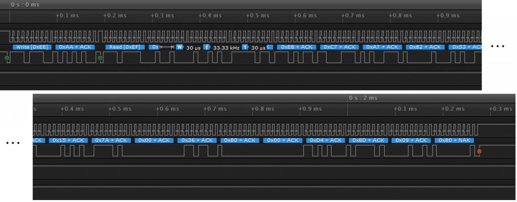
You might notice that the clock in the above trace is a bit asymmetrical. I’m reasonably sure this is down to my use of different value pull-up resistors on SCL and SDA (I settled for ‘close enough’!).
Links
Links: these are from my current browser tabs, they all seem relevant or useful in some way. Some are specific to the SoC rather than the Nano board, so bear this in mind when reading pin configurations etc.
Sipeed Links – the board vendor who make the GD32V SoC available to hobbyists.
- http://dl.sipeed.com/LONGAN/Nano – Official file and docs repository.
- http://dl.sipeed.com/LONGAN/Nano/DOC/GD32VF103_User_Manual_EN_V1.0.pdf SoC Registers
- HDK section of the Sipeed docs – dl.sipeed.com/LONGAN/Nano/HDK/h
- Longan Nano Schematic – PDF schematic of the Longan Nano
- LCD Controller Datasheet – SPD096-IPS, (controller ST7735S, datasheet V1.5)
- https://github.com/sipeed/Longan_GD32VF_examples.git – includes demo gd32v_lcd, with SD card reading (FatFS by ChaN).
GigaDevice Links – the SoC vendor who package the CPU with peripherals and RAM/Flash, etc.
- GigaDevice Documentation and Download Site – Official docs and libraries, English and Chinese.
- GD32VF103 Datasheet Rev 1.1 – Original SoC Datasheet (mechanical & electrical characteristics)
- GD32VF103 User Manual EN V1.1 – Peripheral register definitions
- Firmware Library User Guide V1.0 – peripheral libraries documentation
- https://github.com/riscv-mcu/GD32VF103_Firmware_Library – a treasure trove of peripheral examples, though I think there errors (in the I2C transmitter example, at least).
Nuclei Links – their Bumblebee core is the CPU of the SoC, based on RISC-V spec v2.2.
- Bumblebee Core Concise Datasheet – Overview of the RISC-V core features, ECLIC, and TIMER, and clocks.
- Bumblebee Core Instruction Architecture Manual – Detailed core datasheet.
RISC-V Links – the font of all knowledge, not always in terse and unreadable form.
- RISC-V 101 – Excellent RISC-V primer by SiFive – the PDF slides are linked, and there’s also a webinar presentation.
- https://riscv.org/specifications/ – the official source of RISC-V specifications.
- https://content.riscv.org/wp-content/uploads/2017/05/riscv-spec-v2.2.pdf – RISC-V Instruction Set (2017)
- https://content.riscv.org/wp-content/uploads/2019/06/riscv-spec.pdf – RISC-V Instruction Set (2019)
- https://www.sifive.com/blog/all-aboard-part-4-risc-v-code-models – esp. mention of
--save-tempsto see GCC asm. - https://people.eecs.berkeley.edu/~krste/papers/riscv-privileged-v1.9.1.pdf – Includes CSR register definitions.
- RISC-V Reference Card – PDF cheat sheet of RISC-V (non-pseudo) instructions.
- RISC-V Assembly Programmer’s Manual – Official RISC-V asm programming guide.
- RISC-V Software Status – List of simulators, compilers, bootloaders, IDEs, etc.
Build, Examples, and Miscellaneous stuff
- https://docs.platformio.org/en/latest/installation.html – Installation instructions of CLI tool.
- GCC’s Assembler Syntax – a digestible summary of the
asmstatement. - https://github.com/sipeed/platform-gd32v/tree/master/examples/longan-nano-blink
- https://github.com/sipeed/platform-gd32v/tree/master/examples/arduino-blink
- https://github.com/sipeed/Longan-DOC/blob/master/en/get_started/blink.md – Getting started with IDE.
- https://github.com/LiteOS/LiteOS_PortingContest/tree/master/PortingContest_GD32F103VCT6_ChengXiaoxia_01
- https://github.com/riscv-mcu/gd32-dfu-utils – forked dfu-utils modified for gd32.
- http://nic.vajn.icu/PDF/STMicro/ARM/STM32F1/STM32F10x_USB_devkit.pdf – DFU reference.
- http://www.reactivated.net/writing_udev_rules.html – detailed description of udev rules.
- https://github.com/Kevin-Sangeelee/gd32v_test – a test of LCD, timer, interrupts largely assembled from other examples.
Output from lsusb -v
Bus 001 Device 025: ID 28e9:0189
Device Descriptor:
  bLength                18
  bDescriptorType         1
  bcdUSB               2.00
  bDeviceClass            0 (Defined at Interface level)
  bDeviceSubClass         0
  bDeviceProtocol         0
  bMaxPacketSize0        64
  idVendor           0x28e9
  idProduct          0x0189
  bcdDevice           10.00
  iManufacturer           1 GDMicroelectronics
  iProduct                2 GD32 0x418 DFU Bootloade
  iSerial                 3 䌳䩂  (Note, this is actually 3CBJ)
  bNumConfigurations      1
  Configuration Descriptor:
    bLength                 9
    bDescriptorType         2
    wTotalLength           36
    bNumInterfaces          1
    bConfigurationValue     1
    iConfiguration          0
    bmAttributes         0xc0
      Self Powered
    MaxPower              100mA
    Interface Descriptor:
      bLength                 9
      bDescriptorType         4
      bInterfaceNumber        0
      bAlternateSetting       0
      bNumEndpoints           0
      bInterfaceClass       254 Application Specific Interface
      bInterfaceSubClass      1 Device Firmware Update
      bInterfaceProtocol      0
      iInterface              4 @Internal Flash  /0x08000000/512*002Kg
    Interface Descriptor:
      bLength                 9
      bDescriptorType         4
      bInterfaceNumber        0
      bAlternateSetting       1
      bNumEndpoints           0
      bInterfaceClass       254 Application Specific Interface
      bInterfaceSubClass      1 Device Firmware Update
      bInterfaceProtocol      0
      iInterface              5 @Option Bytes  /0x1FFFF800/01*016 g
      Device Firmware Upgrade Interface Descriptor:
        bLength                             9
        bDescriptorType                    33
        bmAttributes                       11
          Will Detach
          Manifestation Intolerant
          Upload Supported
          Download Supported
        wDetachTimeout                    255 milliseconds
        wTransferSize                    2048 bytes
        bcdDFUVersion                   1.1a
Device Status:     0x0001
  Self Powered
Base Addresses extracted from headers.
The following list of addresses was extracted from the various header files and shows the defines by their bus/peripheral/device hierarchy.
   1 define APB1_BUS_BASE       (0x40000000)
   2         BKP_BASE              (APB1_BUS_BASE + 0x00006C00)
   3         CAN_BASE              (APB1_BUS_BASE + 0x00006400)
   4         DAC_BASE              (APB1_BUS_BASE + 0x00007400)
   5         FWDGT_BASE            (APB1_BUS_BASE + 0x00003000)
   6         I2C_BASE              (APB1_BUS_BASE + 0x00005400)
   7         I2C1                          (I2C_BASE + 0x00000400)
   8         PMU_BASE              (APB1_BUS_BASE + 0x00007000)
   9         RTC_BASE              (APB1_BUS_BASE + 0x00002800)
  10         SPI_BASE              (APB1_BUS_BASE + 0x00003800)
  11         SPI0                          (SPI_BASE + 0x0000F800)
  12         SPI2                          (SPI_BASE + 0x00000400)
  13         TIMER_BASE            (APB1_BUS_BASE + 0x00000000)
  14         TIMER0                        (TIMER_BASE + 0x00012C00)
  15         TIMER1                        (TIMER_BASE + 0x00000000)
  16         TIMER2                        (TIMER_BASE + 0x00000400)
  17         TIMER3                        (TIMER_BASE + 0x00000800)
  18         TIMER4                        (TIMER_BASE + 0x00000C00)
  19         TIMER5                        (TIMER_BASE + 0x00001000)
  20         TIMER6                        (TIMER_BASE + 0x00001400)
  21         USART_BASE            (APB1_BUS_BASE + 0x00004400)
  22         UART3                         (USART_BASE+(0x00000800))
  23         UART4                         (USART_BASE+(0x00000C00))
  24         USART0                        (USART_BASE+(0x0000F400))
  25         USART2                        (USART_BASE+(0x00000400))
  26         WWDGT_BASE            (APB1_BUS_BASE + 0x00002C00)
  27
  28 define APB2_BUS_BASE       (0x40010000)
  29         ADC_BASE              (APB2_BUS_BASE + 0x00002400)
  30         ADC1                          (ADC_BASE + 0x400)
  31         EXTI_BASE             (APB2_BUS_BASE + 0x00000400)
  32         AFIO_BASE             (APB2_BUS_BASE + 0x00000000)
  33         GPIO_BASE             (APB2_BUS_BASE + 0x00000800)
  34         GPIOA                         (GPIO_BASE + 0x00000000)
  35         GPIOB                         (GPIO_BASE + 0x00000400)
  36         GPIOC                         (GPIO_BASE + 0x00000800)
  37         GPIOD                         (GPIO_BASE + 0x00000C00)
  38         GPIOE                         (GPIO_BASE + 0x00001000)
  39
  40 define AHB1_BUS_BASE         (0x40018000)
  41         CRC_BASE              (AHB1_BUS_BASE + 0x0000B000)
  42         DMA_BASE              (AHB1_BUS_BASE + 0x00008000)
  43         DMA1                          (DMA_BASE + 0x0400)
  44         FMC_BASE              (AHB1_BUS_BASE + 0x0000A000)
  45         RCU_BASE              (AHB1_BUS_BASE + 0x00009000)
  46         USBFS_BASE            (AHB1_BUS_BASE + 0x0FFE8000)
  47
  48 define FLASH_BASE            (0x08000000)
  49 define OB_BASE               (0x1FFFF800)
  50 define SRAM_BASE             (0x20000000)  // SRAM0 base
  51 define AHB3_BUS_BASE         (0x60000000)
  52 define EXMC_BASE             (0xA0000000)
  53 define DBG_BASE              (0xE0042000)
  54
  55 define NAND_FLASH_BASE_ADDRESS       0x08010000
  56 define EXT_IO_BASE                   0x40000000 // APB1_BUS_BASE
  57 define USBHS_REG_BASE                0x40040000
  58 define USBFS_REG_BASE                0x50000000
  59 define DRAM_BASE                     0x80000000
  60 define ECLIC_ADDR_BASE               0xd2000000
Hi Kevin,
great write-up. Thanks for compiling this information, it is very useful. Received my Longan today, but it took me some hours to figure out that there is currently no support for MacOS. The PlatformIO packages contain only toolchains for WIndows and Linux. There seems to be an older version available with:
platformio platform install https://github.com/riscv-mcu/platform-gd32v
But I could not get this to work. Will try in a Linux VM ….
What I also do not get is section 4 on https://longan.sipeed.com/en/get_started/blink.html “Connect to the development board”. In the first paragraph they mention upload_protocol = serial for ISP download, in the 3rd section “USB DFU download” upload_protocol = dfu
It confuses me that they “download” while I want “upload” firmware. But more important: Is the first option “serial” used when I upload via UART Rx and TX pins? Or is there a way to get a virtual UART port via USB port on the board?
I run a Linux VM (Debian) Win7 host via VirtualBox. It works great, and the wider support is better than Windows these days, probably more so for MacOS. I do have a Mac here if you ever need something verified.
The board can use DFU, Serial, or JTAG for programming the flash. I have so far only used DFU. The terminology for DFU is the reverse of common conventions, in that it’s from the point of view of the device (which is running the DFU host) to which your client connects. So you ‘upload’ the flash to read it, and ‘download’ to write it.
Although I haven’t used serial yet, I would fairly confidently say that serial programming must be done via TX/RX pins on the board. I’ve seen nothing to suggest that the USB port offers any virtual port. When running the bootloader (holding BOOT0 during reset), both DFU and Serial programming are available.
Thanks for clarification. The documentation is very brief if you start looking into this for the first time. I also would appreciate if they clearly mention that Mac is not supported instead of just letting users into a cryptic error message. But okay I also see that this early bird experimenting and they see the consequences already (many bug reports: https://github.com/sipeed/platform-gd32v/issues/6)
I switched now to Manjaro Linux in a VM. And after switching to DFU mode with boot button and changing the udev rule I was able to upload a the Blink example. After flashing the firmware dfu-util still reports an error (something must go wrong in the very last steps). But this does not matter much.
Will try now to play with the LCD screen. And interestingly with the stock firmware the LED was blinking in three colors, Blink example only shows red. Not sure if this is somewhere documented how to address the other colors.
Glad to hear you made progress. Yes, you have to do a lot of digging and filtering to make sense of the board, but as I see it, everything exists to make it work. For example, you could build the toolchain and modified dfu-utils without too much difficulty to get your own MacOS build. There are proprietary products where this might never be possible.
The warning that dfu-utils reports relates to a missing checksum that will soon (so it says) become mandatory. It’s not there, hence the warning is emitted. There is a way to add the checksum to your firmware file before sending to the device, it’s somewhere on the internet if you care to search.
If you look at my test program on GitHub that is at the bottom of the ‘Links’ section on this page, you can see some code that blinks all three colours in the LED – I took this from another example elsewhere, but I forget which.
Hi Kevin,
Nice post! I’m just about to play with this board, but I’m not enough familiar with the Platformio IDE.
I manage to make blink a LED with DFU mode to upload firmware. Same for the LCD, I can print text on it, it works.
Now, I need to use the CDC_ACM middle-ware to interact with a terminal + USB-C cable and the board. But I have some compilation issues. From what I understood, all the examples I found under file “GD32VF103_Firmware_Library_V1.0.1.rar” use some unknown resources in the SDK.
Example of compilation issues for the GD32VF103_Firmware_Library_V1.0.1\Examples\USBFS\USB_Device\CDC_ACM sample code:
In file included from C:\users\016747\.platformio\packages\framework-gd32vf103-sdk\GD32VF103_usbfs_driver\Include/drv_usb_hw.h:38,
from src\gd32vf103_hw.c:35:
include/usb_conf.h:39:10: fatal error: gd32vf103v_eval.h: No such file or directory
–> if I search in the “GD32VF103_Firmware_Library_V1.0.1.rar” archive the missing header “gd32vf103v_eval.h”, then add it to the “Include” folder of the current project, it goes further, but again hangs:
In file included from C:\users\016747\.platformio\packages\framework-gd32vf103-sdk\GD32VF103_usbfs_driver\Include/drv_usb_regs.h:38,
from C:\users\016747\.platformio\packages\framework-gd32vf103-sdk\GD32VF103_usbfs_driver\Include/drv_usb_core.h:38,
from C:\users\016747\.platformio\packages\framework-gd32vf103-sdk\GD32VF103_usbfs_driver\Include/usbd_core.h:39,
from C:\users\016747\.platformio\packages\framework-gd32vf103-sdk\GD32VF103_usbfs_driver\Include/usbd_enum.h:38,
from include/cdc_acm_core.h:38,
from src\cdc_acm_core.c:35:
include/usb_conf.h:91:10: error: #error “USB_HS_CORE or USB_FS_CORE should be defined”
91 | #error “USB_HS_CORE or USB_FS_CORE should be defined”
| ^~~~~
include/usb_conf.h:103:10: error: #error “USE_USB_HS or USE_USB_FS should be defined”
103 | #error “USE_USB_HS or USE_USB_FS should be defined”
| ^~~~~
If I define manually USE_USB_HS (it’s really ugly, I know 🙂 ), it finish the compilation stage, but this time this is the linker who failed:
c:/users/016747/.platformio/packages/toolchain-gd32v/bin/../lib/gcc/riscv-nuclei-elf/9.2.0/../../../../riscv-nuclei-elf/bin/ld.exe: .pio\build\sipeed-longan-nano\src\cdc_acm_core.o: in function `cdc_acm_init’:
cdc_acm_core.c:(.text.cdc_acm_init+0x16): undefined reference to `usbd_ep_setup’
And this time I’m stuck! The weird things is that it doesn’t complain at all for the “usbd_ep_setup” at compiling stage. And I can find this function “usbd_ep_setup” somewhere in the SDK. I don’t understand why Platformio doesn’t link it.
If you have an idea of what happen here, I would appreciate your help.
Cheers,
Phil
I haven’t built any of the USB examples yet, so I can’t offer any specific help. I would build with ‘-v’ (e.g. platformio run -v …) and check what files are being compiled when it’s building the framework library. If you don’t see usbd_core.c in the compiler output, then the build system doesn’t think you need it. Check that you’ve defined USE_USB_HS in the correct place (I’d also try with FS to see if that affects which files are compiled).
The file gd32vf103v_eval.h is where I’d put project-wide defines. Note that this file is meant to be the board-specific configuration; that file is intended for the GigaDevice evaluation board. See Sipeed’s equivalent in their LCD demo for their modified version. As I recall, the file defines pin wirings for buttons and LEDs, I don’t recall any board specific USB configurations.
First of all, thanks for your post here. Information about this board is hard to find.
You can compile these Examples using Nuclei Studio (Eclipse). Took me a while to realize they don’t work directly with platformio. (I had to switch to use the GD DFU tool, not dfu-util, because that didn’t work with eclipse.)
Examples should build directly with PlatformIO. I don’t use the IDE version, just the command line core that the IDE is built on, and it works well. Check the Sipeed forum for the Longan Nano, there’s quite a lot of useful information there, including build environments. Also, join the Telegram group https://t.me/sipeed
Great article and very good explanations!
Last week I found that jlink supports this board as well. So maybe this link helps other makers as well who want to undust their old Jlink Edu 😉
https://wiki.segger.com/SiPeed_Longan_Nano
Hi,
Thanks for your advices. I’ve test them all, but all failed. While dig deeper and deeper here is what I’ve found in the Platformio board definition :
libs = [
env.BuildLibrary(
join(“$BUILD_DIR”, “standard_peripheral”),
join(FRAMEWORK_DIR, “GD32VF103_standard_peripheral”)),
# env.BuildLibrary(
# join(“$BUILD_DIR”, “usbfs_driver”),
# join(FRAMEWORK_DIR, “GD32VF103_usbfs_driver”)),
env.BuildLibrary(
join(“$BUILD_DIR”, “RISCV”),
join(FRAMEWORK_DIR, “RISCV”)),
]
What a nice joke! If I uncomment those 3 lines, nothing is building. So I guess the Chinese needs to works a little on the USB features :).
I’ll use the USART and add a serialUSB module. It’ll do the job for my needs.
Thanks again for sharing your experiences. Cheers!
Phil
Hi Kevin,
I just got a Longan Nano and installed Visual Studio Code with Platformio add-on.
I used the platformio.ini lines for the arduino blink example:
[env:sipeed-longan-nano]
platform = gd32v
framework = arduino
board = sipeed-longan-nano
monitor_speed = 115200
upload_protocol = dfu
Compiled: ok. Set Longan in download state. I updated the driver (using Windows 10 driver update), so that a USB device called GD32 Device in DFU Mode appears in Device Monitor.
I tried to “download” the Arduino blink example using the USB C with Windows 10 updated drivers and the answer looks positive:
“Download done.
File downloaded successfully
Transitioning to dfuMANIFEST state”
Now comes the question: After Reset, NO sign of blink. Moreover the display went dark, I guess the loaded code erased the initial status.
I have also tried using GD32 MCU Dfu Drivers_v1.0.1.2316 and GD32 MCU Dfu Tool_v3.8.1.5784, I download the firmware.bin with success, as indicated by the Tool.
Being the first time I try to use this board, I would appreciate a suggestion to make work the first code!
Thanks in advance,
MVP
I have pasted the follow-up that you posted on the forum where you answer your own question. Well done figuring it out. I did not know there is a ‘Lite’ version of the Nano.
Thank you for the example I am trying it and modifying it as I go on my Longan Nano board. In your gdv32_test project in main.c what does the statement enable_mcycle_minstret(); do?
It is declared as extern uint32_t enable_mcycle_minstret(); but I am not finding anything else in the project nor is the function described in GD32VF103 firmware library user guide.
In the RISC-V instruction set manual mycycle is defined as ‘machine cycle counter’ and minstret as ‘machine instructions-retired counter’ but I am still not sure how to use it nor how it fits into your program. mcycle looks interesting it seems to be number of instructions executed, I am printing the lower 32 bits of it to LCD and it increases and quickly rolls over.
Right before the closing brace of the while(1) loop I put in a sleep mode instruction that puts the CPU asleep until interrupt, which seems to come from the timer. It slows down the action a lot but makes it more interesting.
pmu_to_sleepmode(WFI_CMD);
Thanks.
This is defined in
RISCV/env_Eclipse/start.S, and is documented in the Bumblebee Core datasheet (section 7.5.1). The counter refers to ‘Instructions Retired’ and is a counter of successfully executed instructions.I think I enabled it simply to get some changing hex values while trying to figure out reading of CSRs. I don’t recall if it’s still even relevant – the code was just written as somewhere to prod the hardware and see the result!
HI,
just ordered a Longan Nano and waiting for it to arrive now… 🙂
Short question: Is there any code to talk to the DAC?
And: On the internet (and some docs I think) I saw mentioned
that there are two DACs as I found information about ony one DAC.
What is “the truth” 🙂 behind it?
I haven’t looked at the DAC registers of the datasheet, nor the wiring on the schematic. Between these docs, you should be able to find an answer. Also, Sipeed have a Telegram group that you can join – it’s the kind of question that you’d likely get a quick answer to. Visit https://t.me/sipeed though the forum is also useful, if a little quiet.
The Nano’s DAC is something on my list (other priorities pushing in!). Do post your project to the Telegram group when you get started; I might join in testing etc.